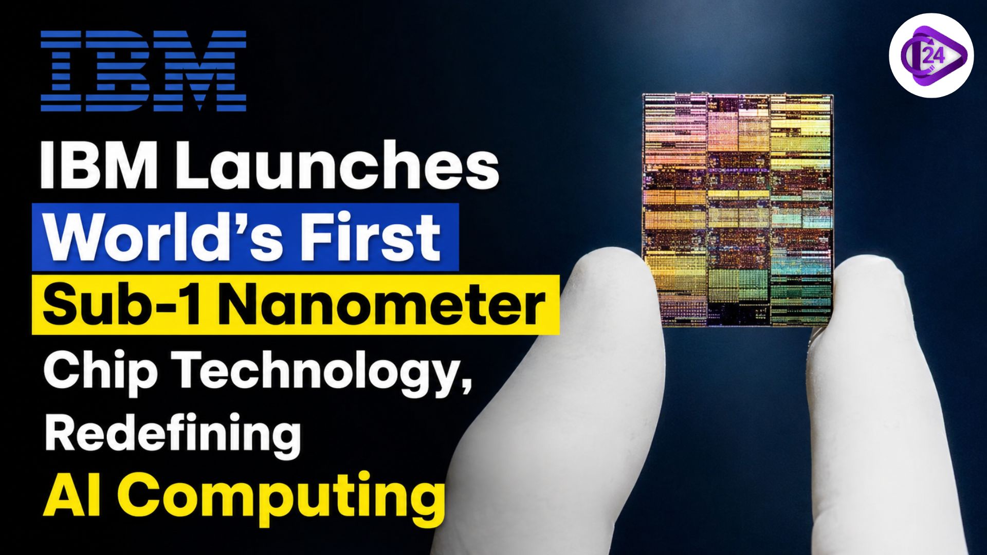
Nanometer Chip: The introduction of IBM Sub-1 Nanometer Chip Technology is one of the biggest breakthroughs in semiconductor manufacturing technology. As AI technologies leap, running on huge amounts of computing power to smaller, faster and more efficient chips, chip makers are exploring how to achieve all these goals. The IBM technology just announced does exactly that, and it’s significantly smaller, with transistor structures even sub-nanometer. This accomplishment enables billions of transistors to be compacted within a very small area, enhancing computing efficiencies, too.
Key Highlights of IBM Sub-1 Nanometer Chip Technology
- IBM has just announced the development of the world’s first Sub-1 Nanometer Chip Technology.
- The breakthrough takes the semiconductor technology over the prevailing 2nm and 1nm boundaries.
- The technology is based on new materials and innovative transistor structures.
- It is intended to be a strong boost to AI computing capabilities.
- The chip enables high-speed processing in a more energy-efficient manner.
- IBM plans to go beyond the current AI models and support quantum computing and high-performance computing in the future.
- The innovation might change the semiconductor industry, as we know it.
- The tech unlocks new use cases in data centres, cloud computing, and edge AI.
How IBM Advanced Semiconductor Technology Works Nanometer Chip
- To boost computing powers while consuming less power, IBM relies on advanced designs for its transistors.
- In technology, they’re trying to fit more transistors in a smaller footprint of the chip to achieve more processing power.
- Novel materials for semiconductors are investigated to see how electricity is used and how much energy is wasted.
- Ultra-small transistor structures can be designed using extremely precise manufacturing techniques.
- Enhanced AI, cloud and high-performance computing tasks are powered by optimised chip designs.
- Many benefits exist with the improved thermal management in high-intensity processing.
- Research is the scope to grow semiconductors beyond the boundaries of normal scale.
- IBM innovations can be used to create faster, energy-efficient processors to power new computing uses.
Best Previous Year Questions
| Year | Exam | Question | Options | Answer |
| 2023 | SSC CHSL | Which of the following materials is most commonly used in semiconductor chip manufacturing? | A. CopperB. SiliconC. IronD. Aluminium | B. Silicon |
| 2022 | SSC CGL | Which of the following is a semiconductor material? | A. SilverB. GoldC. SiliconD. Copper | C. Silicon |
| 2022 | RRB NTPC | The CPU (Central Processing Unit) of a computer primarily consists of: | A. Vacuum TubesB. Semiconductor ChipsC. Magnetic TapesD. Relays | B. Semiconductor Chips |
| 2021 | SSC JE (Electrical) | Which of the following is a semiconductor material? | A. CopperB. SiliconC. SilverD. Iron | B. Silicon |
| 2021 | RRB JE | Which technology is widely used for fabricating integrated circuits used in processors? | A. CMOSB. LCDC. OLEDD. CRT | A. CMOS |
| 2020 | SSC CPO | Which of the following materials is used as the base material for manufacturing most integrated circuits? | A. SiliconB. AluminiumC. CopperD. Iron | A. Silicon |
| 2019 | RRB Group D | A microprocessor used in computers is manufactured using: | A. Semiconductor ChipsB. Vacuum TubesC. Electromechanical RelaysD. Capacitors | A. Semiconductor Chips |
| 2018 | SSC MTS | Which company is globally known for developing advanced semiconductor and computing technologies? | A. IBMB. NokiaC. KodakD. Xerox | A. IBM |
Government Proposes New Indices with 2024–25 Base Year
About IBM: History, Business and Innovation
International Business Machines (IBM) is one of the big American multinational technology companies established on 16 June 1911, and is based in Armonk, New York, USA. It is headquartered in the United States and specialises in artificial intelligence (AI), quantum computing, enterprise software, semiconductor research, hybrid cloud computing and cybersecurity. IBM’s research division is behind several innovations underway and developed, including the world’s first 2-nanometer chip technology, which was announced in 2021. It is also known for its AI platform – IBM Watson, and its quantum computing program named IBM Quantum. Under the leadership of CEO Arvind Krishna, IBM is pushing the boundaries of innovation in next-generation computing, sustainable technology and enterprise digital transformation.
Conclusion on Nanometer Chip
IBM Sub-1 Nanometer Chip Technology is another great innovation in the semiconductor industry. IBM has shown a new way to compute by manipulating transistors smaller than a nanometer. The technology offers faster processors, more energy efficient and higher AI speed. The development is promising, as it could potentially reach the commercial market and further research is required, but it demonstrates the possibilities of semiconductor research in the next generations. With the increasing demand for artificial intelligence, cloud computing, and high-performance computing, IBM Sub-1 Nanometer Chip Technology is likely to have a significant impact on the future of computing worldwide.