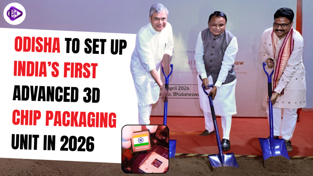
The state of Odisha is to create the first highly effective chip packaging plant in India, and this act will be a significant milestone in the semiconductor journey in India. This is an ongoing project backed by the Government of India and encompasses state-of-the-art 3D heterogeneous integration technology, and is supposed to reinforce the domestic manufacturing of electronics in the country. It was started in Bhubaneswar with the involvement of Bhubaneswar leaders such as Ashwini Vaishnaw. The facility will help drive innovation, curtail import dependence, and make India a competitive entity in the global semiconductor market by making substantial investments and partnering with the world.
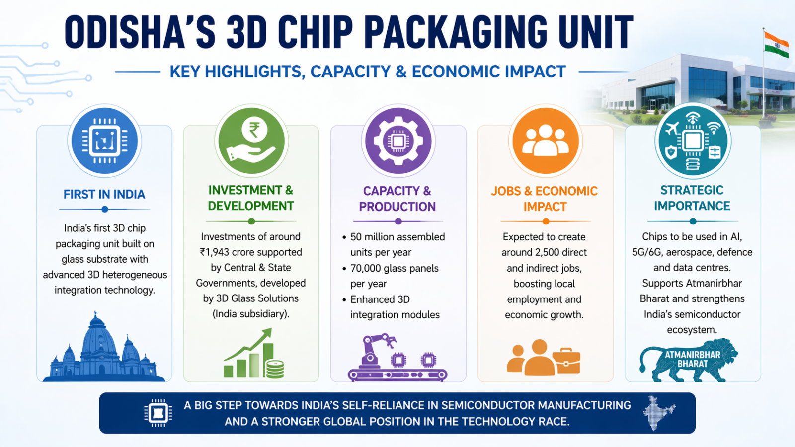
Odisha’s 3D Chip Packaging Unit: Key Highlights, Capacity & Economic Impact
-
It is the first and the latest 3D chip packaging project in India, designed on the basis of the glass substrate.
-
It is under development in Bhubaneswar, rendering Bhubaneswar an important hub of semiconductors.
-
The facility employs new semiconductor packaging technology that is the next generation, 3D heterogeneous integration (3DHI).
-
The investment in the project is approximately 1,943 crore, which is aided by the central and state governments.
-
It is being done by 3D Glass Solutions in its Indian subsidiary.
-
The semiconductor unit production will be 50 million assembled units per year.
-
It will also manufacture 70,000 glass panels in a year and improve 3D modules of incorporation.
-
Approximately 2,500 direct and indirect jobs are projected to be created with the project, which will enhance local employment.
-
The chips produced will be applied in industries such as AI, 5G/6G, aerospace, defence and data centres.
-
The project complies with the government’s vision of Atmanirbhar Bharat.
-
Odisha is the first Indian state to have a semiconductor fabrication and a 3D packaging plant.
-
The project enhances the semiconductor value chain in India and minimises importation.
-
It will be appealing to international technology investments and collaborations ahead.
-
The facility will enable new technologies such as artificial intelligence and high-performance computing.
Recently Asked PYQs on Semiconductor
Question: Which of the following materials is commonly used as a semiconductor? (UPSC Prelims)
A. Copper
B. Silicon
C. Aluminium
D. Iron
Answer: B. Silicon
Explanation: Silicon is the most widely used semiconductor material due to its suitable electrical conductivity and abundance.
Question: The conductivity of a semiconductor increases with: (SSC CGL)
A. Decrease in temperature
B. Increase in temperature
C. Constant temperature
D. No relation
Answer: B. Increase in temperature
Explanation: In semiconductors, higher temperature increases charge carriers, thus increasing conductivity.
Question: Which of the following is an example of a p-type semiconductor? (RRB NTPC)
A. Pure Silicon
B. Silicon doped with Boron
C. Germanium only
D. Copper
Answer: B. Silicon doped with Boron
Explanation: P-type semiconductors are formed by doping with trivalent elements like boron.
Question: What is the function of a diode in semiconductor devices? (SSC CHSL)
A. Amplify signal
B. Store energy
C. Allow current in one direction
D. Increase resistance
Answer: C. Allow current in one direction
Explanation: Diodes permit current flow in only one direction, used in rectification.
Question: Which element is used for n-type doping? (UPSC CDS)
A. Boron
B. Gallium
C. Phosphorus
D. Aluminium
Answer: C. Phosphorus
Explanation: Pentavalent elements like phosphorus provide extra electrons, forming n-type semiconductors.
Question: Semiconductor devices are widely used in: (SSC GD)
A. Agriculture only
B. Electronics
C. Construction
D. Textile
Answer: B. Electronics
Explanation: Semiconductors are the backbone of all electronic devices like mobiles, computers, chips.
Question: Which of the following has the highest conductivity? (UPSC Prelims)
A. Insulator
B. Semiconductor
C. Conductor
D. None
Answer: C. Conductor
Explanation: Conductors have maximum free electrons, hence highest conductivity.
Question: What is the band gap in semiconductors? (UPSC)
A. Zero
B. Very large
C. Small
D. Infinite
Answer: C. Small
Explanation: Semiconductors have a small band gap, allowing controlled conductivity.
Question: Which device is made using semiconductors? (RRB Group D)
A. Transformer
B. Transistor
C. Generator
D. Motor
Answer: B. Transistor
Explanation: Transistors are semiconductor devices used for amplification and switching.
Question: India’s semiconductor mission is related to?
A. Agriculture
B. Electronics manufacturing
C. Defence only
D. Space research
Answer: B. Electronics manufacturing
Explanation: India Semiconductor Mission focuses on chip manufacturing and reducing import dependency.
India Targets Cocoa Self-Sufficiency by 2040
Conclusion – India’s First 3D Chip Packaging Unit in Odisha
The first state-of-the-art 3D chip packing plant in Odisha will be a breakthrough in the Indian ecosystem of semiconductors. The project will increase domestic production through the use of cutting-edge packaging technology and decrease the dependence on imports. It is anticipated to enhance innovation, generate jobs and draw in overseas investments. All in all, this project offers India more strength in the world electronics value network and relates to the dream of technological independence and economic prosperity.